Single-scan AOI, PL and colorimetric analysis support quality control from wafer screening to panel integration
WEVE participated in MicroLED Connect 2026, held on September 16–17 at the High Tech Campus in Eindhoven, the Netherlands. As a Gold Exhibitor, WEVE exhibited and delivered a technical presentation introducing its Bandi MicroLED inspection system and integrated inspection technology.
Jointly organized by the MicroLED Industry Association and TechBlick, the conference and exhibition addressed MicroLED manufacturing and applications alongside AR/VR Connect and Optical I/O Connect. According to the post-event report, attendance increased by more than 25% from the previous year, with keynote presentations from global companies including Sony, Meta, Google and Microsoft.
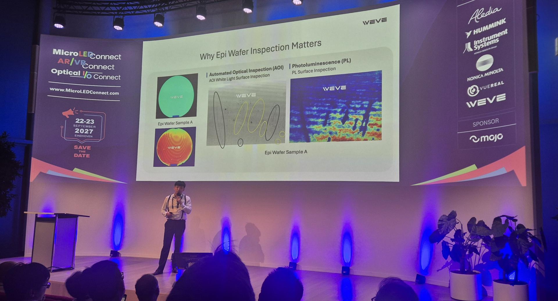
Dmitriy Kim of WEVE presented “Multimodal MicroLED Inspection: From Wafer Screening to Panel Integration.” The presentation explored defect detection and traceability across epitaxial wafers, Chip-on-Wafer (CoW), Chip-on-Carrier (CoC) and final panel integration. Practical examples included identifying weak or non-emitting chips and using inspection maps to prevent defective chips from advancing to subsequent process stages.
Bandi combines automated optical inspection (AOI), photoluminescence (PL) inspection and colorimetric analysis (x, y, Y) in a single scan. The 3-in-1 solution supports simultaneous RGB chip inspection and can inspect a six-inch wafer containing approximately nine million RGB MicroLED chips in under ten minutes, improving inspection efficiency and providing data for yield analysis.
The presentation also explained the need for complementary inspection data throughout manufacturing. Chips that appear acceptable under optical inspection may reveal emission abnormalities through PL analysis, while chips screened at earlier stages still require checks for cracks after transfer and integration. Combining structural and emission data with individual chip locations supports investigation of defects across the manufacturing flow.
During the event, WEVE welcomed MicroLED manufacturers and technology developers from Europe, the United States and other markets to its booth. Discussions covered applications in manufacturing processes and potential technical collaboration, providing an opportunity to exchange perspectives on inspection and quality control for MicroLED production.
Learn More About Bandi